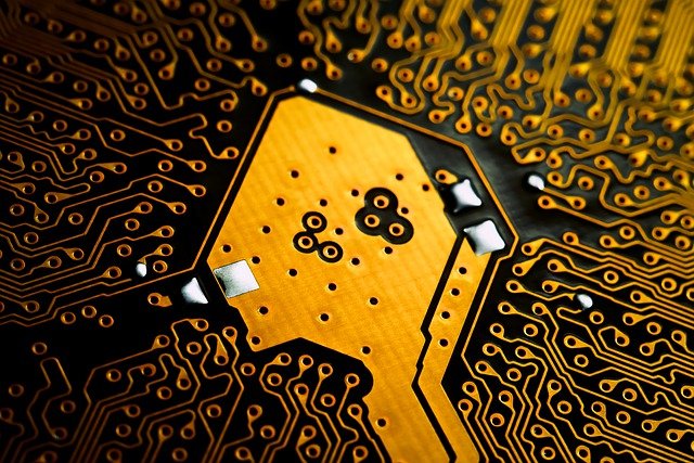
After going through the importance of PCB, you have finally thought of designing one for your use. Adhering to the major PCB designing rule is vital for developing one higher speed based printed circuit board. Working with the right design rules will actually prevent some of the unwanted PCB delays and costs.
While trying to develop that newer PCB design, it is pretty vital to ignore some of the designer rules as that will take most of time concentrating on major circuit design and component selection. If you fail to obey the rule as it has been asked for, it might lead to creation of some poorer design from the physical reality to that current digital domain.
If you want to tailor-made the basic PCB as per your satisfactory level, you need to follow some of the right guidelines for the same. The design rules are further categorized under multiple heads and based on various sections.
Focusing on the board based guidelines:
These guidelines, in particular, are actually linked up with the restrictions of the major board’s size, shape and some of the design aspects, which will influence the design or concept of PCB.
- It will actually entail selection of the reference center, which will benefit the current PCB based manufacturing procedure.
- The main reason for that is to procure holes or reference points on boards, which are then employed for the text fixtures and also for placing and picking machines.
- You also get the chance to enable enough board ground for the current circuit. In some instances, the dimensions of the boards are elucidated by size of product. But, before manufacturing the designs, the board size is to be kept in mind.
- It is vital for you to evaluate the layers beforehand, which are needed for developing PCB right at the start of the design in here. In case you have to include some extra layers, then the production cost in total will hike up. It is vital to ponder ways on how PCB needs to be mounted at start of design
The final layout guidelines:
The entire layout of the PCB design is to be checked before for starting the work on the main design. You can cover that task by drawing and then overviewing layout of where the circuits are to be located.
One of the major parts of the layouts is to draw one rough layout of where the major elements are likely to be based. This form will help to run some of the major tracks right along, while deciding on the best design in here.
Working your way out for the thermal issues:
Even for some of the smaller sized PCBs thermal problems, the issues won’t be that big. But, if you are dealing with some of the higher processing speed and higher component densities of the modern PCBs, then issues are likely to arise. During that time, the thermal issue will be a huge hurdle for you to consider. So, the rule in here is to allow enough space for the hot parts or the PCB components to take time and cool down.
Design based guidelines for the track:
When it comes to tracks on the PCB, those are stated to be initial stage as they are mainly trade-offs. It is mainly vital in case you are pondering over the standard track width, which will then balance the size of the track as well. A short can easily occur in case the track used for it is too close or even too narrow. In the alternative mode, in case the tracks remain wide apart, it might easily influence the number of the track.
Check out all the designs first:
Right from the components used for PCB to the number of layers, you need to focus on everything before dealing with the right design for PCB. Don’t forget to go through all the designs first and then you can make the necessary decision on the choice to make. The more you research, the better choices are subject to be working in your favor. So, waste no time and get along with the best expert for impressive help now.